Cutting Edge Imaging Solutions Customized for Your Needs
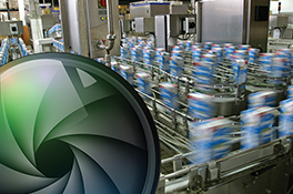
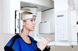
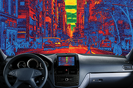
Tower Semiconductor advanced and proven CMOS image sensor technology meets the growing demand for optical sensors used in industrial, medical, high-end photography, automotive and consumer applications, including high end smartphones 3D cameras.
Tower Semiconductor’s worldwide recognized leadership in CMOS image sensors and pixel technology is derived from its vast experience and proven ability to supply sensors with best-in-class performance, customized to fit exactly your products and applications needs.
We provide our customers with robust, reliable manufacturing capabilities combined with unique customizations enabling unmatched pixel design performance with no compromise on quality. The company’s extensive expertise in the imaging field combined with in-house CIS technology development enables Tower Semiconductor to meet the market’s rigorous requirements for leading-edge performance, advanced features, and versatile die sizes, from millimeter square devices to full 12’’ wafer scale single dies.
Tower Semiconductor’s long-term investment in R&D and technical support keeps it at the cutting edge of CIS technology. By choosing Tower Semiconductor’s mature process, customers benefit from skilled experts who work to customize designs and provide rich solutions to meet their requirements and project needs. Tower puts a very strong emphasis on customer support and accompany its partners through the entire product life cycle.
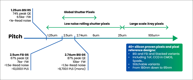
Tower Semiconductor’s CIS technology is offered on three different platforms:
8” wafers, 180nm with aluminum backend – Frontside and Backside illumination and Stacked to 180nm or 130nm
12” wafers, 65nm with copper backend – Frontside and Backside illumination and Stacked Stitching technology is available on both 180nm and 65nm platforms, BSI and FSI and on some stacking options (both two-mask and one-mask stitching).
Core Technology Node
Wafer Size
Backend
BSI/FSI
Stiching
Note
180nm
8’’
Al
BSI/
FSI
1D/2D
180nm stacked
8’’
Al
BSI
Stacked to 180nm or 65nm with coring
65nm
12″
Cu
FSI/ BSI
1D/2D
65nm stacked
12″
Cu
BSI
1D/2D to 65nm
Stacking to multiple nodes, including 3rd party digital wafers
Submit the form below to be contacted by a Tower Semiconductor rep.
Tower Semiconductor websites place cookies on your device to give you the best user experience. By using our websites, you agree to the placement of these cookies. Click to Learn more